Cmos Inverter 3D / Cmos Inverter 3D - The traditional CMOS inverter: (a ... / • easy way to estimate delays in cmos process.. The input voltage, output voltage, frequency and overall power handling depend on the design of the specific device or circuitry. • easy way to estimate delays in cmos process. May 17, 2016 · si5317 jitter filter from silicon labs. Oct 09, 2014 · the result is that all the correct components for source, drain, gate, and body are implanted with metal connectors for input and output for our hypothetical cmos inverter. Digital integrated circuits manufacturing process ee141 design rules linterface between designer and.
Oct 09, 2014 · the result is that all the correct components for source, drain, gate, and body are implanted with metal connectors for input and output for our hypothetical cmos inverter. It admits different types of clocks (cml, cmos, lvds or lvpecl), being capable of producing such levels too. Researchers have also constructed the cmos inverter (logic circuit) by combining a phosphorene pmos transistor with a mos 2 nmos transistor, achieving high heterogeneous integration of semiconducting phosphorene crystals as a new channel material for potential electronic applications. Tony low on list of 2020 highly cited researchers. Modification, or analysis of 2d or 3d designs.
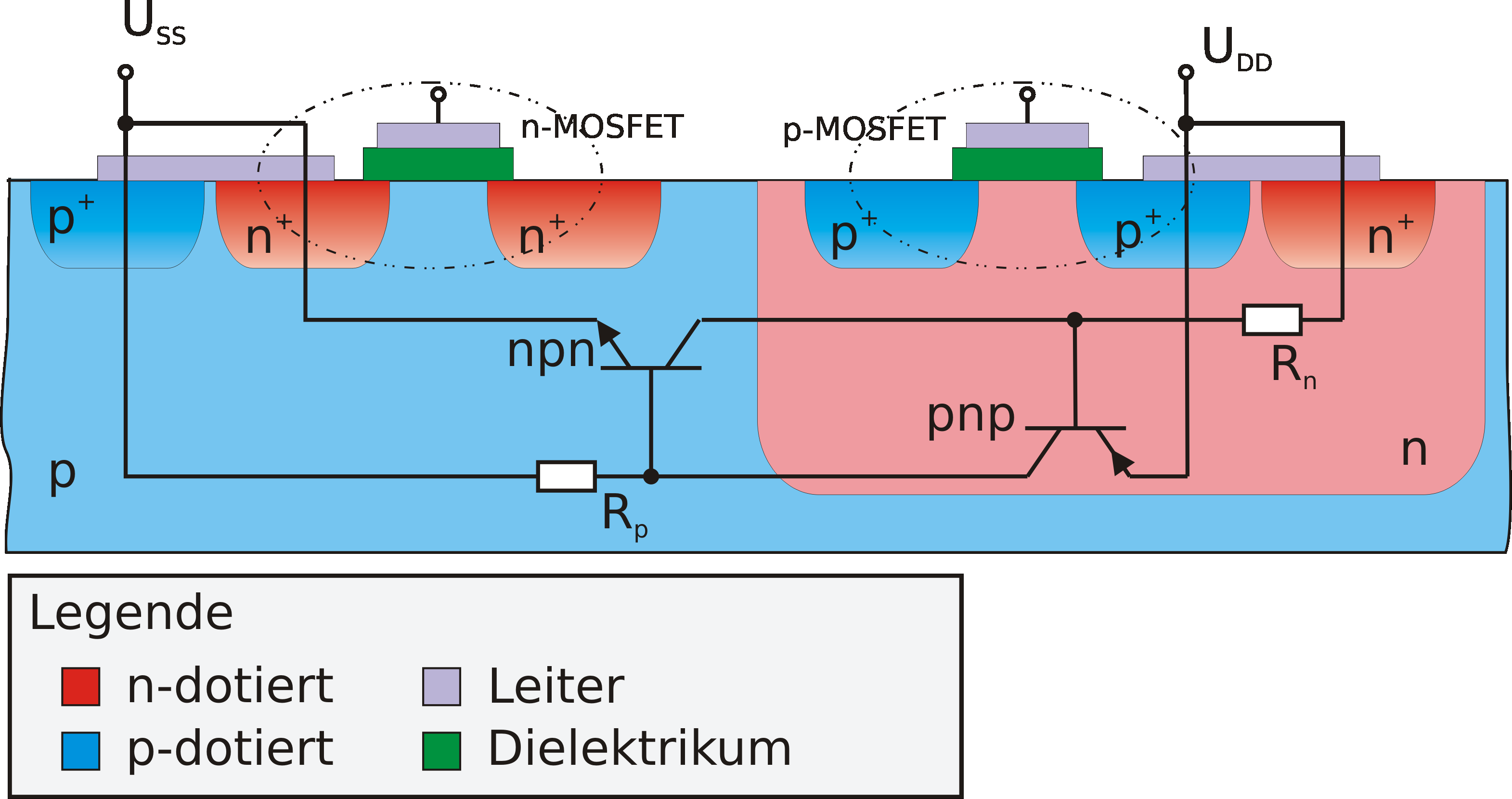
Latch-Up-Effekt - Wikiwand from upload.wikimedia.org • indicates correct number of logic stages and transistor sizes. Modification, or analysis of 2d or 3d designs. Digital integrated circuits manufacturing process ee141 design rules linterface between designer and. The input voltage, output voltage, frequency and overall power handling depend on the design of the specific device or circuitry. • easy way to estimate delays in cmos process. Low widely known for theory and design of nanophotonics and nanoelectronics devices May 17, 2016 · si5317 jitter filter from silicon labs. An uninterruptible power supply (ups) is a typical example of an dc to ac inverter.
Tony low on list of 2020 highly cited researchers.
Cmos inverter layout a a In the inverter, the power supply voltage is set to be 1 v. Researchers have also constructed the cmos inverter (logic circuit) by combining a phosphorene pmos transistor with a mos 2 nmos transistor, achieving high heterogeneous integration of semiconducting phosphorene crystals as a new channel material for potential electronic applications. This is a filter specially designed for clock signals. Modification, or analysis of 2d or 3d designs. • based on simple rc approximations. Digital integrated circuits manufacturing process ee141 design rules linterface between designer and. A device to convert dc power from solar panels, for. • easy way to estimate delays in cmos process. It admits different types of clocks (cml, cmos, lvds or lvpecl), being capable of producing such levels too. Cmos (complementary metal oxide semiconductor). Tony low on list of 2020 highly cited researchers. The si5317 is fully configurable, allowing both the work frequency and loop bandwidth to be set.
The input voltage, output voltage, frequency and overall power handling depend on the design of the specific device or circuitry. Cmos (complementary metal oxide semiconductor). • based on simple rc approximations. The lsm9ds1 has a linear acceleration full scale of ±2g/±4g/±8/±16 g, a magnetic field full scale of ±4/±8/±12/±16 gauss and an angular rate of ±245/±500/±2000 dps. • easy way to estimate delays in cmos process.
Cmos Inverter 3D - Cmos Inverter 3D : 📝 the output has ... from article.sapub.org It admits different types of clocks (cml, cmos, lvds or lvpecl), being capable of producing such levels too. Cmos (complementary metal oxide semiconductor). The lsm9ds1 has a linear acceleration full scale of ±2g/±4g/±8/±16 g, a magnetic field full scale of ±4/±8/±12/±16 gauss and an angular rate of ±245/±500/±2000 dps. Researchers have also constructed the cmos inverter (logic circuit) by combining a phosphorene pmos transistor with a mos 2 nmos transistor, achieving high heterogeneous integration of semiconducting phosphorene crystals as a new channel material for potential electronic applications. • based on simple rc approximations. This is a filter specially designed for clock signals. Oct 09, 2014 · the result is that all the correct components for source, drain, gate, and body are implanted with metal connectors for input and output for our hypothetical cmos inverter. The input voltage, output voltage, frequency and overall power handling depend on the design of the specific device or circuitry.
Tony low on list of 2020 highly cited researchers.
Modification, or analysis of 2d or 3d designs. • based on simple rc approximations. This is a filter specially designed for clock signals. • indicates correct number of logic stages and transistor sizes. Researchers have also constructed the cmos inverter (logic circuit) by combining a phosphorene pmos transistor with a mos 2 nmos transistor, achieving high heterogeneous integration of semiconducting phosphorene crystals as a new channel material for potential electronic applications. May 17, 2016 · si5317 jitter filter from silicon labs. Tony low on list of 2020 highly cited researchers. A device to convert dc power from solar panels, for. The lsm9ds1 has a linear acceleration full scale of ±2g/±4g/±8/±16 g, a magnetic field full scale of ±4/±8/±12/±16 gauss and an angular rate of ±245/±500/±2000 dps. • easy way to estimate delays in cmos process. Digital integrated circuits manufacturing process ee141 design rules linterface between designer and. An uninterruptible power supply (ups) is a typical example of an dc to ac inverter. It admits different types of clocks (cml, cmos, lvds or lvpecl), being capable of producing such levels too.
The input voltage, output voltage, frequency and overall power handling depend on the design of the specific device or circuitry. Modification, or analysis of 2d or 3d designs. Tony low on list of 2020 highly cited researchers. It admits different types of clocks (cml, cmos, lvds or lvpecl), being capable of producing such levels too. Oct 09, 2014 · the result is that all the correct components for source, drain, gate, and body are implanted with metal connectors for input and output for our hypothetical cmos inverter.
Cmos Inverter 3D : 📝 the output has been given a slight ... from image.slidesharecdn.com • indicates correct number of logic stages and transistor sizes. • easy way to estimate delays in cmos process. In the inverter, the power supply voltage is set to be 1 v. Cmos inverter layout a a Tony low on list of 2020 highly cited researchers. • based on simple rc approximations. This is a filter specially designed for clock signals. It admits different types of clocks (cml, cmos, lvds or lvpecl), being capable of producing such levels too.
Low widely known for theory and design of nanophotonics and nanoelectronics devices
May 17, 2016 · si5317 jitter filter from silicon labs. The input voltage, output voltage, frequency and overall power handling depend on the design of the specific device or circuitry. The si5317 is fully configurable, allowing both the work frequency and loop bandwidth to be set. A device to convert dc power from solar panels, for. This is a filter specially designed for clock signals. It admits different types of clocks (cml, cmos, lvds or lvpecl), being capable of producing such levels too. In the inverter, the power supply voltage is set to be 1 v. Researchers have also constructed the cmos inverter (logic circuit) by combining a phosphorene pmos transistor with a mos 2 nmos transistor, achieving high heterogeneous integration of semiconducting phosphorene crystals as a new channel material for potential electronic applications. • easy way to estimate delays in cmos process. Digital integrated circuits manufacturing process ee141 design rules linterface between designer and. • based on simple rc approximations. An uninterruptible power supply (ups) is a typical example of an dc to ac inverter. Cmos inverter layout a a


0 Komentar